{var%20f='http://v.t.sina.com.cn/share/share.php?appkey=1515056452',u=z||d.location,p=['&url=',e(u),'&title=',e(t||d.title),'&source=',e(r),'&sourceUrl=',e(l),'&content=',c||'gb2312','&pic=',e(p||'')].join('');function%20a(){if(!window.open([f,p].join(''),'mb',['toolbar=0,status=0,resizable=1,width=440,height=430,left=',(s.width-440)/2,',top=',(s.height-430)/2].join('')))u.href=[f,p].join('');};if(/Firefox/.test(navigator.userAgent))setTimeout(a,0);else%20a();})(screen,document,encodeURIComponent,'','','https://www.xiaopingtou.cn//data/attach/topic/topicKPo7gB.jpg', '推荐 神話 的文章《NXP(Freescale) QorIQ T2080 IFC》','https://www.xiaopingtou.cn/article-64098.html','页面编码gb2312|utf-8默认gb2312'));)
class="markdown_views prism-dracula">


参考RM 13.4.1.2.1,T2080RDB-PC采用Mode 0,地址复用时数据总线上为地址的MSB,功能框图,因为是16位的NOR,所以A26不使用,对于8位的NOR,A26接A0。Latch由74LVC16373锁存器完成。

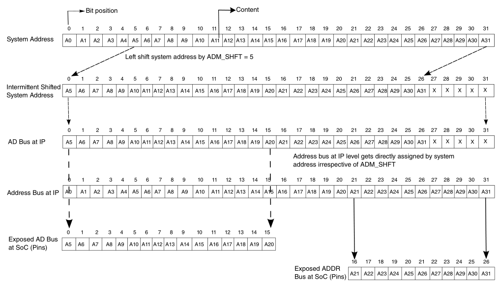
地址转换流程,ADM_SHIFT=5,和T2080RDB-PC是对应的,及从A5到A30,A31悬空。
启动时的ADM_SHIFT由cfg_rcw_src决定,

而T2080RDB-PC的值为11,所以有32位的寻址能力。启动后ADM_SHIFT由IFC_CSORn_NOR寄存器决定,可以移动0到20位。

看下T2080RDB-PC的image分布,通过控制原理图中的CFG_VBANK0脚从0到1(CFG_VBANK1=0,CFG_VBANK2=0),切换0xE8xxxxxx到0xECxxxxxx(异或关系),这儿的CPU寻址的高地址出现在了低地址线。

RCW在0xE8000000,这是uboot看到的,估计也是内核看到的,这点从uboot代码可以看出,FLASH的基址在0xE8000000,CONFIG_SYS_NOR_AMASK是128MB,符合硬件设计,

NOR启动不需要uboot spl,但T2080 CPC SRAM位512KB,不够装载uboot,所以代码在Nor中本地运行(in place),AMASK作用是定义一个Memory BANK的大小,参考RM,寄存器IFC_AMASKn的低16位不使用,所以最小的BANK为64KB(最小分配单位),也就是说,即使你占用的空间不到64KB,IFC也得分配64KB,下面的公式阐述了系统地址(40位空间用到CSPRn_EXT寄存器)和IFC地址(32位)的关系,可以看到cpu访存的高地址出现在了低地址了,位反序了。

读时序,

更改代码,
参考
Device Tree Address Ranges for NOR, NAND & CPLD
[PATCH 2/2] fsl_ifc: Support all 8 IFC chip selects
概述
IFC(Integrated Internal Controller)用于访问异步NAND flash, 异步NOR flash,SRAM, generic ASIC memory和EPROM。T2080RDB-PC的IFC原理图,
NOR
特性:- 支持地址数据复用ADM(address data multiplexed)NOR芯片
- 系统复位后,启动片选为CS0
- 数据宽度为8或16bits
参考RM 13.4.1.2.1,T2080RDB-PC采用Mode 0,地址复用时数据总线上为地址的MSB,功能框图,因为是16位的NOR,所以A26不使用,对于8位的NOR,A26接A0。Latch由74LVC16373锁存器完成。
地址转换流程,ADM_SHIFT=5,和T2080RDB-PC是对应的,及从A5到A30,A31悬空。
启动时的ADM_SHIFT由cfg_rcw_src决定,
而T2080RDB-PC的值为11,所以有32位的寻址能力。启动后ADM_SHIFT由IFC_CSORn_NOR寄存器决定,可以移动0到20位。
看下T2080RDB-PC的image分布,通过控制原理图中的CFG_VBANK0脚从0到1(CFG_VBANK1=0,CFG_VBANK2=0),切换0xE8xxxxxx到0xECxxxxxx(异或关系),这儿的CPU寻址的高地址出现在了低地址线。
RCW在0xE8000000,这是uboot看到的,估计也是内核看到的,这点从uboot代码可以看出,FLASH的基址在0xE8000000,CONFIG_SYS_NOR_AMASK是128MB,符合硬件设计,
//T208xRDB.h
#define CONFIG_SYS_FLASH_BASE		0xe8000000
#define CONFIG_SYS_FLASH_BASE_PHYS	(0xf00000000ull | CONFIG_SYS_FLASH_BASE)
#define CONFIG_SYS_NOR0_CSPR_EXT	(0xf)
#define CONFIG_SYS_NOR0_CSPR	(CSPR_PHYS_ADDR(CONFIG_SYS_FLASH_BASE_PHYS) |
				CSPR_PORT_SIZE_16 |
				CSPR_MSEL_NOR |
				CSPR_V)
#define CONFIG_SYS_NOR_AMASK	IFC_AMASK(128*1024*1024)
//cpu_early_init.c
void setup_ifc(void)
{
	...

	/* Change flash's physical address */
	ifc_out32(&(ifc_regs.gregs->cspr_cs[0].cspr), CONFIG_SYS_CSPR0);
	ifc_out32(&(ifc_regs.gregs->csor_cs[0].csor), CONFIG_SYS_CSOR0);
	ifc_out32(&(ifc_regs.gregs->amask_cs[0].amask), CONFIG_SYS_AMASK0);

	return ;
}
CONFIG_SYS_NOR0_CSPR_EXT=0xf,说明手册里标注24-31的,在c语言里是低8位。NOR启动不需要uboot spl,但T2080 CPC SRAM位512KB,不够装载uboot,所以代码在Nor中本地运行(in place),AMASK作用是定义一个Memory BANK的大小,参考RM,寄存器IFC_AMASKn的低16位不使用,所以最小的BANK为64KB(最小分配单位),也就是说,即使你占用的空间不到64KB,IFC也得分配64KB,下面的公式阐述了系统地址(40位空间用到CSPRn_EXT寄存器)和IFC地址(32位)的关系,可以看到cpu访存的高地址出现在了低地址了,位反序了。
BASE_ADDRn[0:23] = {CSPRn_EXT[BA_EXT], CSPRn[BA]}, n=0-7 (chip select)

{BASE_ADDRn[0:7], (BASE_ADDRn[8:23] & AMn[0:15])} ==
{SYSTEM_ADDR[39:32], (SYSTEM_ADDR[31:16] & AMn[0:15])}
libmtd: error!: MEMERASE64 ioctl failed for eraseblock 0 error 5 (Input/output error)
闹心的问题,留着后面解决吧,这应该是内核问题,ioctl传下去返回就错了。root@t2080rdb:~# flash_erase /dev/mtd2 0 0
Erasing 128 Kibyte @ 0 -- 0 % complete libmtd: error!: MEMERASE64 ioctl failed for eraseblock 0 (mtd2)
error 5 (Input/output error)
flash_erase: error!: /dev/mtd2: MTD Erase failure
error 5 (Input/output error)
Erasing 128 Kibyte @ 20000 -- 12 % complete libmtd: error!: MEMERASE64 ioctl failed for eraseblock 1 (mtd2)
error 5 (Input/output error)
flash_erase: error!: /dev/mtd2: MTD Erase failure
error 5 (Input/output error)
Erasing 128 Kibyte @ 40000 -- 25 % complete libmtd: error!: MEMERASE64 ioctl failed for eraseblock 2 (mtd2)
error 5 (Input/output error)
flash_erase: error!: /dev/mtd2: MTD Erase failure
error 5 (Input/output error)
Erasing 128 Kibyte @ 60000 -- 37 % complete libmtd: error!: MEMERASE64 ioctl failed for eraseblock 3 (mtd2)
error 5 (Input/output error)
flash_erase: error!: /dev/mtd2: MTD Erase failure
error 5 (Input/output error)
Erasing 128 Kibyte @ 80000 -- 50 % complete libmtd: error!: MEMERASE64 ioctl failed for eraseblock 4 (mtd2)
error 5 (Input/output error)
flash_erase: error!: /dev/mtd2: MTD Erase failure
error 5 (Input/output error)
Erasing 128 Kibyte @ a0000 -- 62 % complete libmtd: error!: MEMERASE64 ioctl failed for eraseblock 5 (mtd2)
error 5 (Input/output error)
flash_erase: error!: /dev/mtd2: MTD Erase failure
error 5 (Input/output error)
Erasing 128 Kibyte @ c0000 -- 75 % complete libmtd: error!: MEMERASE64 ioctl failed for eraseblock 6 (mtd2)
error 5 (Input/output error)
flash_erase: error!: /dev/mtd2: MTD Erase failure
error 5 (Input/output error)
Erasing 128 Kibyte @ e0000 -- 87 % complete libmtd: error!: MEMERASE64 ioctl failed for eraseblock 7 (mtd2)
error 5 (Input/output error)
flash_erase: error!: /dev/mtd2: MTD Erase failure
error 5 (Input/output error)
Erasing 128 Kibyte @ e0000 -- 100 % complete
GPCM
GPCM接口用于访问CPLD和FPGA的寄存器,优化时序参数,加快ifc读写寄存器速度,写时序,读时序,
更改代码,
/* FPGA on IFC */
#define CONFIG_SYS_FPGA_CS_FTIM0		(FTIM0_GPCM_TACSE(0x0) |
					FTIM0_GPCM_TEADC(0x4) |
					FTIM0_GPCM_TEAHC(0x0))
#define CONFIG_SYS_FPGA_CS_FTIM1		(FTIM1_GPCM_TACO(0x0) |
					FTIM1_GPCM_TRAD(0x1f))
#define CONFIG_SYS_FPGA_CS_FTIM2		(FTIM2_GPCM_TCS(0x0) |
					FTIM2_GPCM_TCH(0x0) |
					FTIM2_GPCM_TWP(0x8))
#define CONFIG_SYS_FPGA_CS_FTIM3		0x0